INSA
The activity of the “Quantum Optoelectronics” team of the Laboratory of Physics and Chemistry of Nano-Objects (LPCNO-INSA, is focused on the study of the electronic and optical properties of semiconductor materials and nanostructures, with significant expertise in the spin physics of electronic states. The research covers a spectrum of activities ranging from basic research to applications and development, with a strong involvement in training through research and teaching.

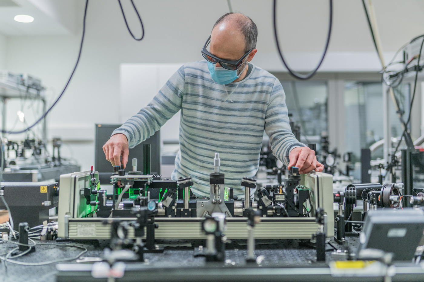
The team’s scientific strategy consists of developing original spectroscopic investigation tools, often combining spatial and temporal resolution, making it possible to analyze novel nano-objects or semiconductor materials.
The fundamental research activity falls within the general issues of spin electronics and quantum technologies, which are the subject of strong international competition. The key expertise of the team concerns the excitonic and optical properties of two-dimensional materials based on transition metal dichalcogenides. We were fortunate to be among the pioneers in this field, in particular thanks to the identification in 2011/2012 of the original spin / valley properties. We have recently made significant advances in particular on the measurement of the binding energy of the exciton, its fine structure (bright and black states), the characteristics of the excited states, the dielectric screening effects, the dynamics of radiative recombination, Auger effects, spin / valley relaxation mechanisms … In addition to stationary or time-resolved optical spectroscopy measurements which are the specialty of the team, strong efforts have been put on the development of sample fabrication benches and device manufacturing. These efforts make it possible to obtain very high quality samples and to have a very rapid process between physical ideas, manufacturing and measurement.
At the same time, the expertise acquired in the team is used in more applied research, in collaboration with public or industrial partners. This is an important asset for this proposal. These research contracts concern in particular: optical telecommunications (band structure engineering for semiconductor amplifiers with Nokia Bell Labs, III-V Lab and APEX Technologies); electronic components for space (study of irradiation effects via the development of ultra-fast laser irradiation benches with the TRAD SME); nanomaterials for photovoltaics and photocatalysis (Cu2ZnSnS4 and WSe2).
By mentioning only the collaborations which gave rise to publications, let us quote at the national level the UMP CNRS-Thales (Palaiseau), the Jean Lamour Institute (Nancy), the LPN (Marcoussis), PMC Polytechnique (Palaiseau), Foton ( Rennes) and at international level: Stanford (USA), Arizona State University (USA), Los Alamos National Lab. (USA), University of Berlin (G), University of Munich (G), University of Regensburg (G), University of Heriot Watt (G.B.); ETH Zurich (Switzerland), Tyndall National Institute (Irl.), University of Milano (It.), University of Warwick (UK), Institut Ioffe (Russia), University Autonoma Metropolitana (Mex.), NIMS Tsukuba (Jap.), Institute of Semiconductors Beijing (China), Institute of Physics Beijing (China).